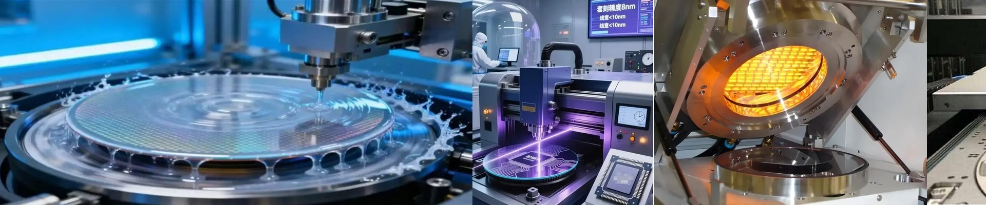
On the fab floor, a half-degree temperature drift during the photoresist bake is the kind of thing that quietly murders yield. Wafers come in with a tight thermal budget, and the heater has to deliver repeatable heat—cycle after cycle—without adding particle risk. What matters, technically We build semiconductor-equipment heaters with wafer-level uniformity of ±0.1°C, measured on the substrate, not on the platen. Fast-ramp short-wave and medium-wave infrared elements, matched to quartz or ceramic bodies, cut soak time and keep profiles stable. Zero particle generation comes from cleanroom-compatible materials and sealed termination design, so Class 1–100 environments stay in spec. And repeatability is engineered in through calibrated sensors and stable drivers, so soft bake and hard bake temperatures stay within tight tolerances across lots. Why it works in lithography In lithography lines, that consistency translates to predictable photoresist profiles, fewer reworks, and tighter CD control. The process window opens up because the thermal profile doesn’t drift with shift changes or line voltage. Energy use drops as rapid setpoint attainment reduces idle soak, and 24/7 reliability keeps unplanned downtime down. The result is higher device yield and stable OEE—two levers that directly move the manufacturing economics. Things to keep straight Matching the heater to the chamber geometry and the clamp/pin contact pattern is non-negotiable. A mismatch creates hot spots and turns wafers into scrap. Expect a short thermal soak-in period after installation while the control loop settles and you verify uniformity maps. And plan calibration intervals that line up with your PM schedule—tighter specs demand more process discipline.